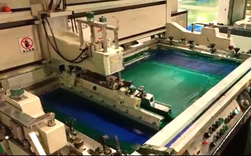
Full Catalog
Engineered
Solutions
Comprehensive product lines catering to advanced printed circuit board manufacturing requirements — from thermal inks to precision tooling.
Comprehensive product lines catering to advanced printed circuit board manufacturing requirements — from thermal inks to precision tooling.
Every product currently in production, ready for sample requests and volume pricing.
 Inks
Inks
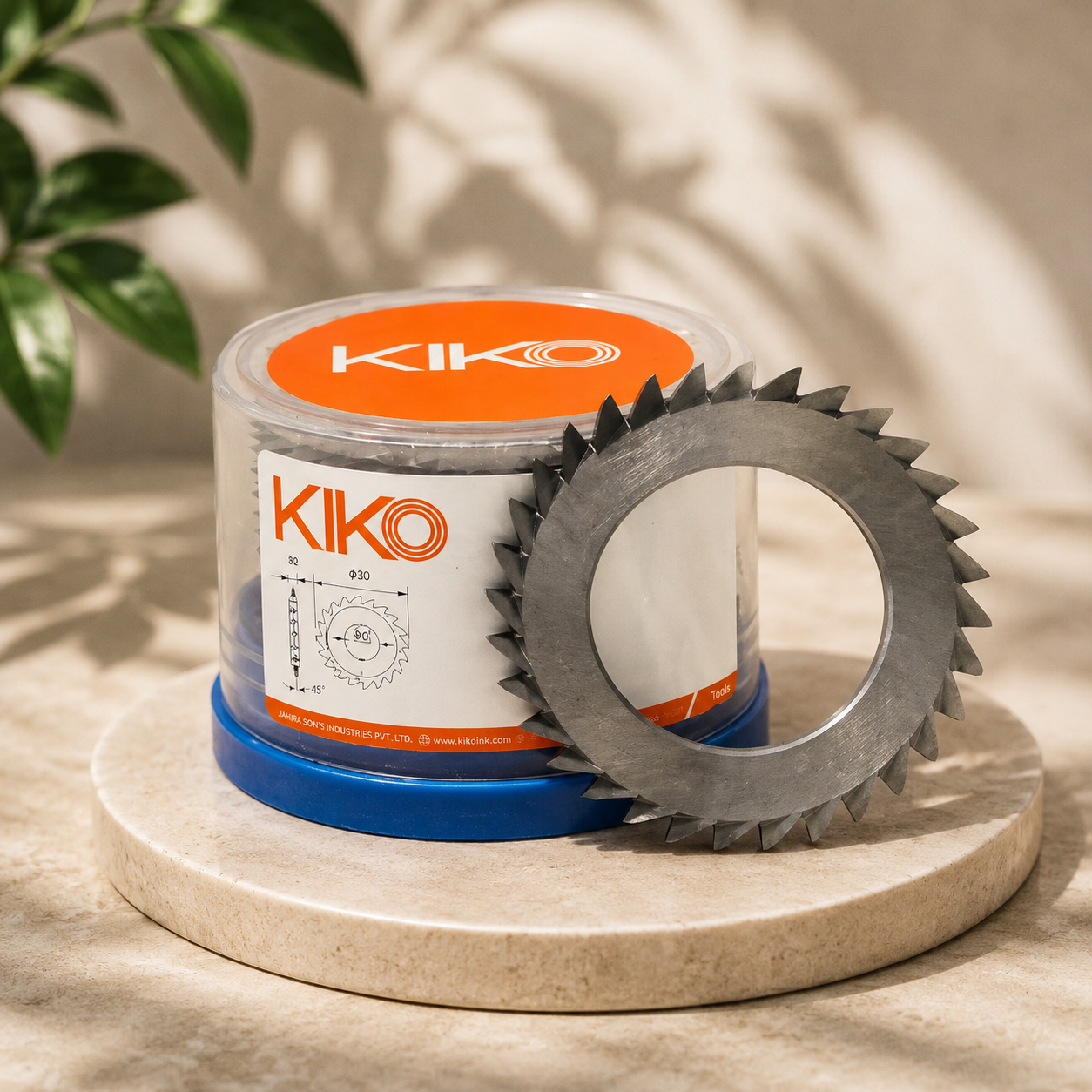
Solid carbide cutter for high-speed, durable PCB board separation.
 Tooling
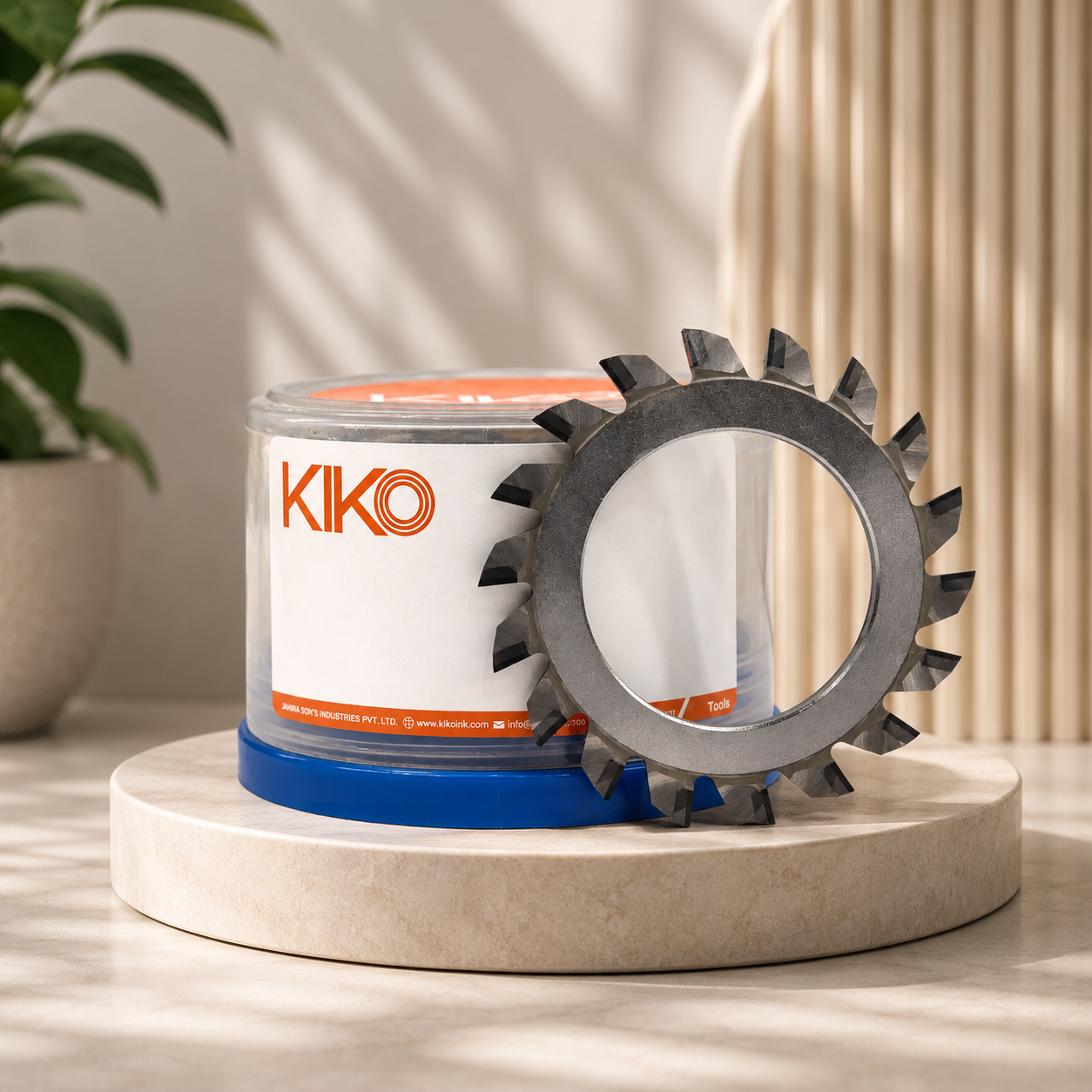
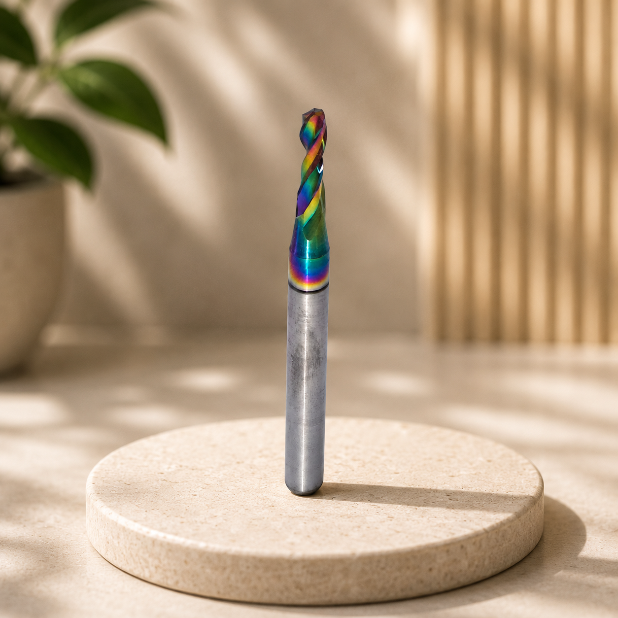
Diamond tip carbide cutter for fine, precise PCB board separation with minimal chipping.
 Inks
Inks
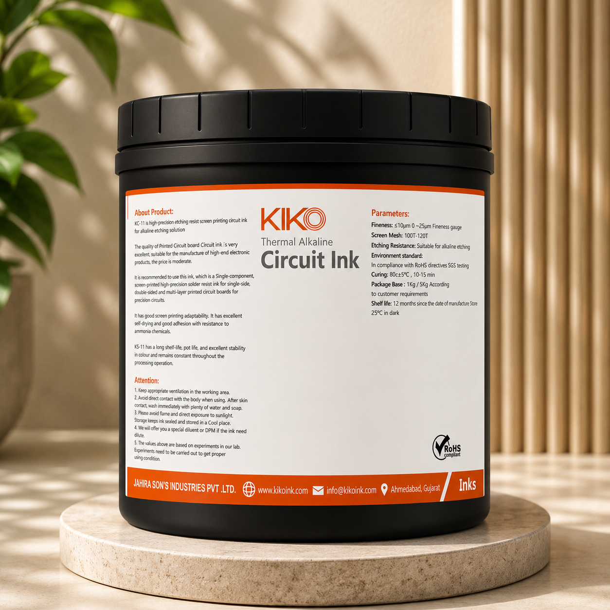
Thermal Alkaline Series for reliable circuit pattern formation on LED PCBs.
 Inks
Inks
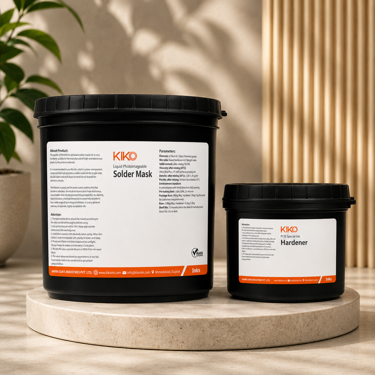
KIKO Liquid Photoimageable (LPI) Solder Mask Ink is a premium UV-curable solder resist designed for high-density and multilayer PCBs.
 Tooling
Precision carbide router bits for clean PCB profiling and edge routing.
 Inks
Inks
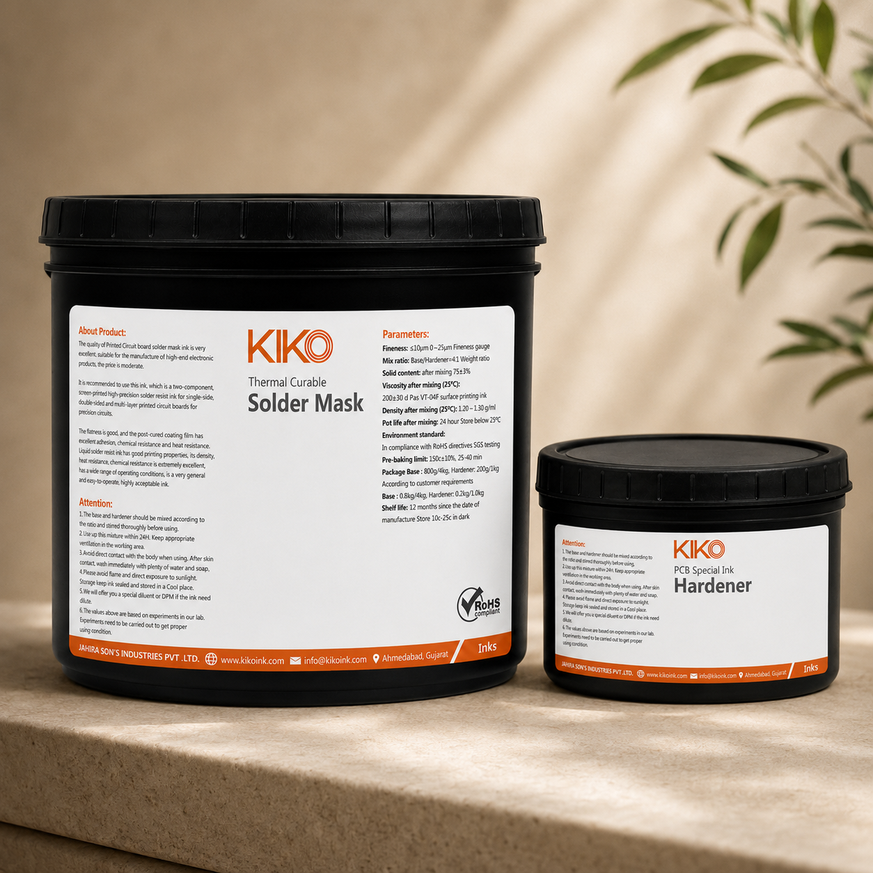
Advanced thermal curable protection for high-performance LED PCBs. Available in Rice White and Blue White.
 Inks
Inks
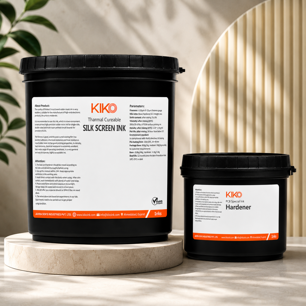
Thermal Curable KS-51 series for high-visibility legends, markings, and component identification on PCBs.
 Tooling
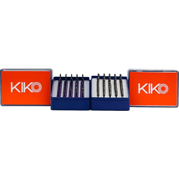
Precision carbide tooling for extreme accuracy and durability in PCB production lines.
Every KIKO formulation is batch-tested against strict tolerances. Switch between products to see how each one is built.
A fast side-by-side view for B2B buyers evaluating multiple products at once.
| Product | Category | Available Colours | Cure / Curing | Download |
|---|---|---|---|---|
| Carbide Cutter (KCT-C32) | Inks | — | — | — |
| Diamond Tip Carbide Cutter (KCT-D18) | Tooling | — | — | — |
| Circuit Ink (KC-11) | Inks | — | TDS PDF → | |
| PISM Liquid Photoimgaable Solder Mask Ink | Inks | — | — | — |
| Router (KRT-PRO) | Tooling | — | — | — |
| Solder Mask Ink (KS-21) | Inks | — | TDS PDF → | |
| Silk Screen Ink (KL-51) | Inks | — | — | |
| Cutter & Drill Bits | Tooling | — | — |
Manufacturers choose KIKO because every batch is formulated for consistency, not just performance on paper. Our thermal, photoimageable, and precision tooling lines are engineered specifically for high-volume PCB production, where a single inconsistent batch can stall an entire line.
Beyond the formulation itself, KIKO works as a technical partner rather than a supplier that simply ships product. Our team reviews your existing process before recommending a specific ink or mask, which reduces trial-and-error during onboarding.
KIKO products are used across circuit formation, solder mask application, legend printing, and precision drilling stages of PCB manufacturing. Circuit inks support both single and multi-layer trace formation with reliable adhesion and resolution.
Solder mask formulations protect copper traces while withstanding soldering heat and long-term field exposure; silk screen inks provide durable, legible component marking; precision drill bits and cutting tools support clean, accurate hole formation.
Every product line moves through a structured internal process before it reaches a customer's line: raw material selection and testing, batch formulation under controlled conditions, in-house quality checks against defined tolerances, and final packaging suited to shelf-life requirements.
This same discipline extends to how we onboard new clients — requirement analysis, product selection, sample testing, mass production, and ongoing technical support.
Our products support PCB manufacturers across automotive electronics, LED lighting, consumer electronics, industrial systems, power supply equipment, and computing hardware.
Each of these sectors places different demands on an ink or coating — from thermal cycling in automotive applications to UV stability in LED lighting — and our formulations are selected or adapted accordingly rather than treated as one-size-fits-all.
Batch consistency is checked against defined tolerances before any product leaves our facility, covering properties like viscosity, adhesion, cure behaviour, and insulation resistance depending on the product type.
For B2B buyers, this means the ink or tooling you validate during sample testing behaves the same way at full production volume — reducing the risk of line stoppages, rework, or rejected boards further down the supply chain.
Our photoimageable inks (PISM and solder mask ranges) are formulated for the fine-line resolution and registration accuracy multilayer boards require. Share your layer count and pad pitch with our technical team for a specific recommendation.
Selection depends on your exposure equipment, board finish, and operating environment. Our team reviews your cure profile and application method, then recommends a colour and formulation from the Solder Mask range accordingly.
Yes. Every product page has a Request Sample option, and our technical team can arrange trial quantities so you can validate performance on your own line before committing to volume.
Please contact our sales team with your destination and required volumes so we can confirm logistics, documentation, and lead times for your order.
TDS PDFs are available for download directly from each product page where published. If a datasheet isn't listed yet for a product you need, contact us and we'll share it directly.
Talk to our technical expert — we'll match a formulation to your line, not the other way around.